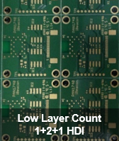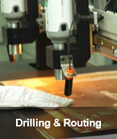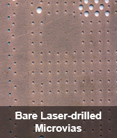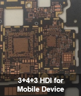
High-Density Interconnects (HDI) process technology has continually evolved into PCB designs since its initial introduction in semiconductor package modules in the late 1980s. Today, drilling laser control depth blind µVias into a variety of laminates, utilizing a variety of copper plating processes, has become the dominant method of HDI fabrication. Multek's extensive qualification methodology assures the reliability of complex µVia structures in a range of laminates that are thermally robust to multiple SMT reflow cycles. Our Material and HDI development roadmaps are focused on continuous feature size reduction for µVias, which is essential for today's cost-sensitive designs.
Multek has been a leader in HDI interconnect innovation and mass production for over fifteen years. All of our factories have mass production capacity for µVia-based HDI processing, combined with fine line copper trace formation by semi-additive or subtractive copper plating.
Click here to view the datasheet.
